Research Stories
Analysis of Atomic Structures and Electrical Characteristics of MoS2
A research team led by Prof. Young Hee LEE from the Institute for Basic Science successfully analyzed atomic structures and electrical characteristics of MoS 2 which are labeled as new materials for the next generation along with Graphene.
Physics
Prof.
LEE, YOUNGHEE
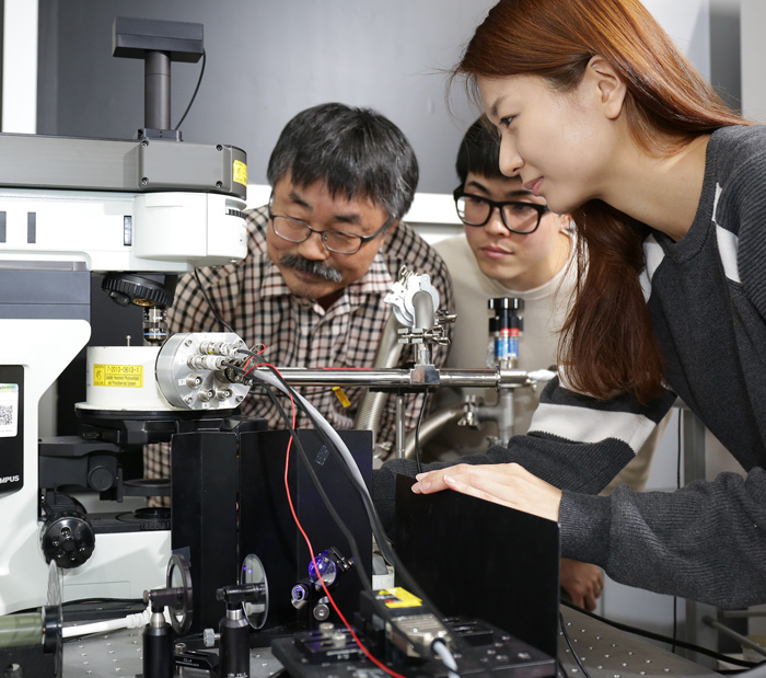
A research team led by Prof. Young Hee LEE from the Institute for Basic Science successfully analyzed atomic structures and electrical characteristics of MoS 2 which are labeled as new materials for the next generation along with Graphene.
Grain boundaries in monolayer transition metal dichalcogenides have unique atomic defect structures and band dispersion relations that depend on the inter-domain misorientation angle. They explored misorientation angledependent electrical transport at grain boundaries in monolayer MoS 2 by correlating the atomic defect structures of measured devices analysed with transmission electron microscopy, and first-principles calculations. Transmission electron microscopy indicates that grain boundaries are primarily composed of 5–7 dislocation cores with periodicity and additional complex defects formed at high angles, obeying the classical low-angle theory. The inter-domain mobility is minimized for angles of 9° and increases nonlinearly by two orders of magnitude before saturating at 16 cm 2 V -1 s -1
around misorientation angle of 20°. This trend is explained via grain-boundary electrostatic barriers estimated from density functional calculations and experimental tunnelling barrier heights, which are 0.5 eV at low angles and 0.15 eV at high angles (≥20°). The results provide practical expectations regarding transport properties in large-area films, which are restricted largely by the poor mobility across low-angle grain boundaries. Also this work is applicable to other similar 2D systems and contribute to the fundamental understanding of transport in semiconductors. This research was published at Nature Communications, affiliated magazine with Nature.
이황화몰리브덴과 그래핀은 나노박막 지름이 수 십 마이크로미터(㎛·1㎛는 100만분의 1m)에 불과한 미세한 입자들이 연결된 형태다. 각 원자의 결합구조 때문에 이웃한 두 결정입자의 각도가 서로 틀어지면서 특이한 경계면(결정립계면)이 생긴다. 결정립계면은 전기의 이동을 방해하기 때문에 반도체 회로 구성에 걸림돌이 돼 왔다. 그러나 이황화몰리브덴의 결정립계면의 형태에 따라 전기적 특성이 어떻게 변하는지 아직까지 알려진 것이 없었다.
연구팀은 고해상도투과전자현미경(HRTEM)을 활용해 각 결정립계면의 틀어진 각도와 원자결합구조 상태를 정밀하게 관측하고, 서로 다른 각도로 틀어진 여러 결정립계면의 전하 이동을 측정했다. 그 결과 이황화몰리브덴도 그래핀처럼 결정립계면에서 전기저항이 높아지고 이에 따라 전하이동도가 떨어지며, 틀어진 각도가 전하이동도에 영향을 준다는 사실이 처음으로 밝혀졌다. 계면의 각도가 8도 정도일 때 전하이동이 가장 낮았고, 8~20도 범위에서는 각도가 커질수록 전하이동도 증가했다. 최종적으로 약 20도 이상에서는 가장 높은 값을 유지했다.
이번 연구 결과에 쓰인 분석 방법은 층상구조를 띤 다른 반도체 물질에도 적용할 수 있을 것이고 이를 토대로 고성능 신소재 반도체를 구현하는 시기를 앞당길 수 있을 것으로 기대한다.
이 성과는 ‘네이처’ 자매지 ‘네이처 커뮤니케이션스’ 에 실렸다.