Research Stories
World’s first discovery of defect-related Raman scattering signal by using tip-enhanced Raman spectroscopy
Research team has detected defect-related Raman scattering signal of monolayer tungsten disulfide using tip-enhanced Raman spectroscopy (TERS).
Energy Science
Prof.
JEONG, MUNSEOK
Researcher LEE, CHANWOO
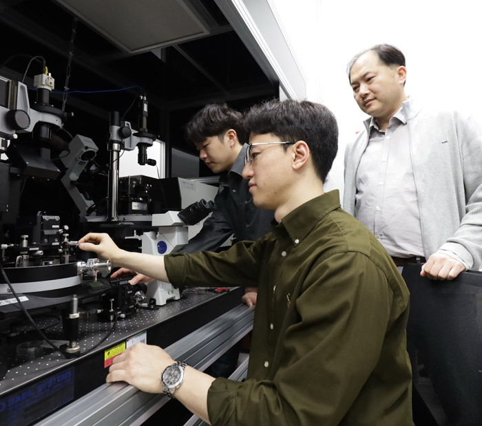

Prof. Mun Seok JEONG’s research team (Department of Energy Science) reported that the defect-related Raman scattering signal was successfully obtained from a monolayer tungsten disulfide by using tip-enhanced Raman spectroscopy.
Two-dimensional transition metal dichalcogenides (TMD) materials have been widely investigated due to their optical properties such as the bandgap engineering that depends on the number of layers. In particular, monolayer tungsten disulfide (WS2) shows intense photoluminescence with a relatively high quantum yield among TMDs. Thus, monolayer WS2 has attracted much interest as an outstanding material for 2D optoelectronic devices.
To achieve the high performance of optoelectronic devices, the defect-free WS2 is highly required. Accordingly, it is necessary to establish a quality evaluation method by investigating the defects of monolayer WS2.
The research team was able to detect new signals in areas with many defects by using tip-enhanced Raman spectroscopy, which can simultaneously perform surface nanostructure analysis and optical measurement. In addition, density functional theory (DFT) calculations confirmed that this signal is attributable to the sulfur atom (S) vacancies. The researchers called it a "D mode" from the defect and reported that it provides a criterion for evaluating the quality of monolayer WS2 compared to the intensity of the signal in the defect-free area.
Prof. JEONG said, “It is notable that this study was the first to detect signals related to defects in two-dimensional semiconductor materials. In the future, it can be applied to various two-dimensional semiconductor materials to determine quality evaluation standards, and it can accelerate the commercialization of two-dimensional semiconductors.
These findings have been published in the journal “ACS Nano (IF = 13.709)” (October 23rd 2018).
This work was supported by IBS-R011-D1 and the National Research Foundation of Korea (NRF) Grant funded by the Korean government (MSIP) (2016R1A2B2015581). Mr. Chanwoo LEE (Ph.D. candidate, Departmentof Energy Science) participated as the lead author and Dr. Seung Mi LEE (Korea Research Institute of Standards and Science) participated as a co-corresponding author.
(Diagram) Measurement of defects